Description
Key Technical Specifications
| Parameter | Value |
|---|---|
| Manufacturer | LAM Research |
| Model | 810-046015-010 |
| Product Type | VIOP III Control PCB Assembly |
| Board Designation | VIOP-3 Board |
| Application | Semiconductor manufacturing equipment |
| Main Function | Equipment control, I/O processing, and internal communication |
| PCB Type | Multi-layer industrial control board |
| Interface | Equipment-specific connectors and control buses |
| Processing Role | Real-time machine subsystem coordination |
| Installation | LAM process equipment control chassis |
| Compatible Equipment | LAM semiconductor etch platforms (configuration dependent) |
| Operating Environment | Semiconductor cleanroom equipment environment |
| Maintenance Category | Legacy semiconductor equipment spare part |
Product Introduction
LAM Research 810-046015-010 Overview
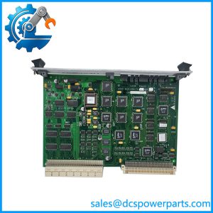
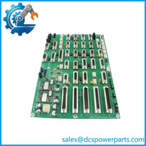
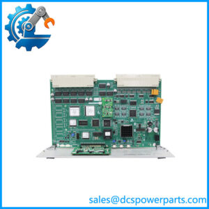
The LAM Research 810-046015-010 is a VIOP III control board assembly used in LAM semiconductor manufacturing equipment. It functions as a machine-level control interface, handling communication between equipment subsystems, field devices, and the main equipment controller. It is identified as a VIOP-3 board used in semiconductor process tools.
The LAM Research 810-046015-010 is typically maintained in installed wafer processing equipment where replacing the complete tool control architecture is not practical. Engineers should verify board revision, equipment software version, connector mapping, and system configuration before installation because semiconductor tools are highly dependent on matched hardware and software combinations.
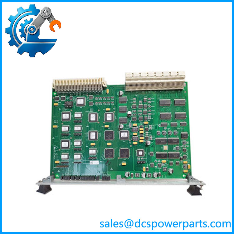
810-046015-010
Application Scenarios & Field Pitfalls (The Engineer’s Perspective)
Engineering Pain Point
A semiconductor process tool can stop production because of a single control board fault. The chamber may be mechanically sound. The vacuum system may pass checks. Yet a failed I/O processor board can interrupt sensor feedback, actuator commands, or subsystem communication.
The LAM Research 810-046015-010 sits inside this control chain. Replacement requires more than installing a PCB and powering up the machine. Configuration recovery is usually the difficult part.
Typical Applications
- Semiconductor Fabrication Plants – Wafer etch equipment control and subsystem communication.
- Advanced Packaging Facilities – Process tool automation and precision equipment management.
- Research Semiconductor Labs – Maintenance of legacy LAM process development systems.
- Microelectronics Manufacturing – Equipment control systems requiring accurate I/O coordination.
Technical Pitfalls to Avoid
- Hardware Revision Verification
LAM equipment often uses similar-looking boards with different firmware requirements or connector assignments. Confirm the complete part number and PCB revision before replacement.
- Software Configuration Recovery
A replacement VIOP board may require equipment-specific configuration files. Always confirm software backup availability before removing the original board.
- ESD and Cleanroom Handling
Semiconductor control boards are sensitive to static discharge and contamination. Use proper ESD procedures and avoid unnecessary exposure during handling.
Field note: Before removing the original board, document slot location, cable routing, LED status, software version, and active alarms. These records are valuable during equipment recovery.
Related Products
- LAM Research 810-046015-010 VIOP III Board
Main replacement reference for existing LAM semiconductor equipment installations. Used for equipment control and I/O processing functions. - LAM Research 810-066590-004
Related LAM interface/control board used in semiconductor equipment architectures. It performs different subsystem interface functions and is not a direct replacement. - LAM Research 810-099175-012
Related LAM control board family component used for analog signal processing applications within semiconductor tools. - LAM Research 810-073479-215
Another LAM equipment control board used in semiconductor manufacturing systems. Compatibility depends on equipment platform and revision. - LAM Research 810-102361-2
Related legacy control board reference used in LAM equipment maintenance applications. - LAM Research 810-068158-014
Interface/control PCB component used within LAM equipment assemblies. - LAM Research 2300 Series Etch Systems
Equipment family associated with various LAM control and process modules. Specific board compatibility depends on chamber configuration. - LAM Research Kiyo Platform
Modern LAM etch equipment family. Legacy board replacements require confirmation of exact tool model and installed hardware configuration. - LAM Semiconductor Equipment Control PCB Assemblies
Specialized electronic assemblies used for machine control, I/O processing, and subsystem communication in wafer fabrication equipment.