Description
GE DS200TCDAH1BHD | Mark V TCDA Digital I/O Board
Key Technical Specifications
| Parameter | Specification |
|---|---|
| Product Model | DS200TCDAH1BHD |
| Manufacturer | GE |
| Product Family | Mark V Speedtronic |
| Board Family | DS200 |
| Functional Acronym | TCDA |
| Product Type | Digital I/O Board |
| Primary Function | Digital contact input/output processing |
| Processor | Onboard microprocessor |
| Programmable Memory | Multiple PROM devices |
| Main Ribbon Connectors | 2 × 50-pin |
| Auxiliary Connectors | 2 × 3-pin, JX1 and JX2 |
| Diagnostic LEDs | 1 × 10-LED block + 1 side-visible LED |
| Hardware Jumpers | 8 |
| Jumper Functions | IONET termination, IONET ID, stall-timer selection, factory-test functions |
| Test Points | TP-designated circuit test points |
| Associated Termination Boards | DS200DTBA / DS200DTBB |
| Associated Relay Boards | TCRA boards |
| Communication | Mark V IONET architecture; not a general-purpose Ethernet I/O module |
| Firmware | Board-dependent PROM configuration |
| Operating Voltage | Verify from installed Mark V cabinet documentation |
| Operating Temperature | Verify against applicable Mark V system documentation |
| Mounting | Mark V control cabinet/rack |
| PCB Coating | Conformal coating |
The documented TCDAH1B hardware uses J2/J3 for IONET termination-resistor selection, J4/J5/J6 for IONET ID selection, and J7 for stall-timer enable. J1 and J8 are identified for factory testing and should not be changed during normal maintenance.
Product Introduction
The GE DS200TCDAH1BHD is a Mark V TCDA Digital I/O Board used for discrete signal processing inside GE Speedtronic turbine-control equipment. The board receives digital contact information through the associated termination hardware and handles digital output information associated with the Mark V control architecture. It is a system-specific control PCB, not a standalone PLC digital-input card.
The TCDA sits between field termination hardware and the Mark V control electronics. Published documentation identifies the two 50-pin interfaces as JQ and JR: JQ connects toward the DS200DTBA termination board, while JR receives contact-input signals associated with DS200DTBB. The board also interfaces with TCRA circuitry for contact-output processing.
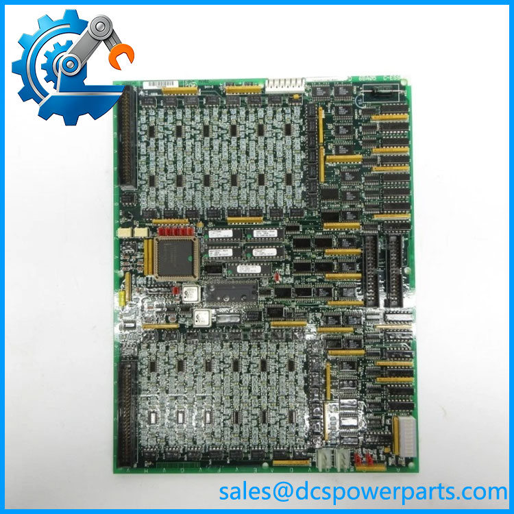
DS200TCDAH1BHD
Engineering Pain Point
A failed TCDA can produce symptoms that look like field wiring or termination-board faults because the board is directly involved in digital signal processing between the Mark V control core and termination hardware. Replacing the PCB without documenting the original jumper configuration can introduce a second problem after the original failure has been removed. The IONET ID, termination settings, and stall-timer selection must be preserved where applicable.
Typical Applications
- GE Mark V turbine control: Processing discrete contact signals within legacy Speedtronic turbine-control cabinets.
- Digital contact monitoring: Handling input information originating from Mark V termination boards.
- Digital output processing: Working with TCRA relay-output circuitry within the Mark V architecture.
- Legacy turbine maintenance: Replacement of failed TCDA hardware while preserving the existing cabinet architecture and configuration.
Technical Pitfalls to Avoid
- Do not treat the BHD suffix as cosmetic. The complete
DS200TCDAH1BHDdesignation should be matched against the removed PCB, including artwork and revision markings. - Record jumper positions before removal. The documented TCDAH1B assembly uses hardware jumpers for IONET termination, IONET ID, stall-timer selection, and factory-test functions.
- Do not change factory-test jumpers casually. J1 and J8 are identified as factory-test positions in the available technical documentation.
- Check the ribbon-cable path. JQ and JR are associated with different termination-board signal paths. Swapping or misrouting ribbon cables can create multiple apparent I/O failures.
- Verify the IONET ID. J4, J5, and J6 are used for the board’s IONET ID selection. A physically correct replacement with the wrong ID configuration can behave incorrectly within the Mark V network.
- Do not use generic PLC I/O specifications. Voltage, temperature, and channel-level ratings found on unrelated modern I/O products should not be applied to this Mark V PCB.
Related Products
- DS200TCDAH1B — Base TCDA Digital I/O Board designation corresponding to the documented B-revision assembly; useful when checking the underlying board family against the complete BHD suffix.
- DS200TCDAG1B — Another Mark V TCDA Digital I/O board configuration; verify connector, revision, and application before considering substitution.
- DS200TCDAG1BDB — Mark V TCDA Digital I/O configuration with a different suffix; not automatically interchangeable with
H1BHD. - DS200DTBA — Digital termination board associated with the TCDA signal path; the TCDA JQ interface connects toward its JQR connector.
- DS200DTBB — Related digital termination board providing another contact-input signal path to the TCDA.
- DS200TCRA — Mark V relay-output circuitry associated with TCDA digital output processing.
- DS200TCCAG1BAA — Mark V analog I/O board with a fundamentally different signal function; not a TCDA replacement.
- DS200TBQAG1ABB — Mark V termination board for a different signal architecture; not interchangeable with a TCDA digital I/O PCB.
- DS200SLCCG3AGH — Mark V LAN communication board; related to system communication but not a digital I/O replacement.
Procurement Note
For a DS200TCDAH1BHD replacement, verify the complete PCB number, functional revision, artwork revision, PROM configuration, jumper positions, connector arrangement, and cabinet/core location. Before removal, photograph J1–J8 and record the JQ/JR ribbon-cable routing.
The available documentation establishes the TCDA digital I/O function and the architecture of the closely matching DS200TCDAH1B assembly, but it does not provide sufficiently reliable suffix-specific voltage, current, or environmental limits for DS200TCDAH1BHD. Those values should be taken from the installed Mark V documentation and board nameplate rather than inferred from a reseller listing.